INTEGRATED CIRCUITS DIVISION
MX884
4
www.ixysic.com
R01
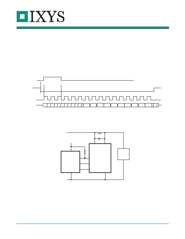
2 Functional Description
The MX884 converts a small voltage developed
across an external sense resistor (Rs) to a 10-bit
digital output. Pin IN connects to the 3V to 60V power
input. The external current sense resistor connects
between pins IN and LOAD. The nominal A/D range is
100 mV V(IN)-V(LOAD) across Rs. The A/D least
significant bit typically equals 0.1 mV across R
S
.
Inputs CS and SCK are TTL-level compatible, 5.5V
maximum input voltage. Inputs can be driven from
CMOS microcontrollers operating at supply voltages
of 2.4 to 5.5V. Serial data output pin SDO is configured
as open drain, maximum 5.5V external pull-up. SCK is
used internally to clock the successive approximation
register of the A/D.
Figure 1. Serial Timing Diagram
Figure 2. Typical Application Circuit
CS
SCK
SDO
D9
D8
D7
D6
D5
D4
D3
D2
D1
D0
Internal S/H
Power
Supply
0.1?/DIV>
10nF
+3V
microcontroller
Power
Return
MX884
GND
SDO
CS
SCK
LOAD
IN
5
1
6
2
4
3
Load
发布紧急采购,3分钟左右您将得到回复。
相关PDF资料
NCP1080DEG
IC CONV CTLR POE-PD 13W 20-TSSOP
NCP1081DEG
IC CONV CTLR POE-PD 40W 20-TSSOP
NCP1082DEG
IC CONV CTLR POE-PD 13W 20-TSSOP
NCP1083DEG
IC CONV CTLR POE-PD 40W 20-TSSOP
NCP1501DMR2G
IC REG SGL BUCK/LINEAR 8MICRO
NCP1578MNR2G
IC REG DL BCK/LINEAR SYNC 20-QFN
NCP1601BDR2G
IC PFC CTRL CRM/TRANSITION 8SOIC
NCP1603D100R2G
IC CTLR PFC/PWM COMBO 16-SOIC
相关代理商/技术参数
MX8870
制造商:未知厂家 制造商全称:未知厂家 功能描述:Controller Miscellaneous - Datasheet Reference
MX887D
制造商:CLARE 制造商全称:Clare, Inc. 功能描述:μPower Hall-Effect Switch
MX887DHT
制造商:IXYS Integrated Circuits Division 功能描述:MX Series 5.5 V 2 mA Surface Mount Power Hall-Effect Switch - TSOT-23-3
MX887DHTTR
功能描述:板机接口霍耳效应/磁性传感器 Power Hall Effect Switch w/Open Drain Output 3-lead TSOT-23 on T&R RoHS:否 制造商:Honeywell 类型:Bipolar Hall-Effect Digital Position Sensor 工作电源电压:3 V to 24 V 电源电流:3.5 mA 最大输出电流:20 mA 工作点最小值/最大值:5 G, 55 G 最小/最大释放点(Brp):- 55 G, - 5 G 最大工作温度:+ 150 C 安装风格:SMD/SMT 封装 / 箱体:SOT-23
MX887P
制造商:CLARE 制造商全称:Clare, Inc. 功能描述:??Power Hall-Effect Switch
MX887PHTTR
功能描述:板机接口霍耳效应/磁性传感器 Power Hall Effect Switch w/Push-Pull Output 3-lead TSOT-23 on T&R RoHS:否 制造商:Honeywell 类型:Bipolar Hall-Effect Digital Position Sensor 工作电源电压:3 V to 24 V 电源电流:3.5 mA 最大输出电流:20 mA 工作点最小值/最大值:5 G, 55 G 最小/最大释放点(Brp):- 55 G, - 5 G 最大工作温度:+ 150 C 安装风格:SMD/SMT 封装 / 箱体:SOT-23
MX88L284AEC
制造商:未知厂家 制造商全称:未知厂家 功能描述:Highly integration chip for Flat Panel Display application
MX88L285-S
制造商:未知厂家 制造商全称:未知厂家 功能描述:Converter